The VLSI Design Flow

The VLSI IC circuits design flow is shown in the figure below. The various level of design are numbered and the gray coloured blocks show processes in the design flow.
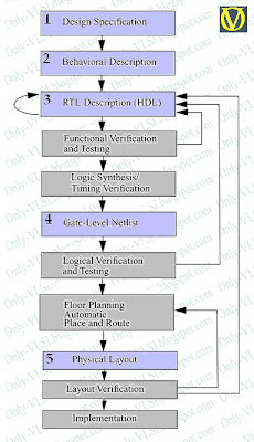
Specifications comes first, they describe abstractly the functionality, interface, and the architecture of the digital IC circuit to be designed.
  • Behavioral description is then created to analyze the design in terms of functionality, performance, compliance to given standards, and other specifications.
  • RTL description is done using HDLs. This RTL description is simulated to test functionality. From here onwards we need the help of EDA tools.
  • RTL description is then converted to a gate-level netlist using logic synthesis tools. A gate-level netlist is a description of the circuit in terms of gates and connections between them, which are made in such a way that they meet the timing, power and area specifications.
  • Finally a physical layout is made, which will be verified and then sent to fabrication.

Comments

Popular posts from this blog

Digital Design Interview Questions - All in 1

1. How do you convert a XOR gate into a buffer and a inverter (Use only one XOR gate for each)? Answer 2. Implement an 2-input AND gate using a 2x1 mux. Answer 3. What is a multiplexer? Answer A multiplexer is a combinational circuit which selects one of many input signals and directs to the only output. 4. What is a ring counter? Answer A ring counter is a type of counter composed of a circular shift register. The output of the last shift register is fed to the input of the first register. For example, in a 4-register counter, with initial register values of 1100, the repeating pattern is: 1100, 0110, 0011, 1001, 1100, so on. 5. Compare and Contrast Synchronous and Asynchronous reset. Answer Synchronous reset logic will synthesize to smaller flip-flops, particularly if the reset is gated with the logic generating the d-input. But in such a case, the combinational logic gate count grows, so the overall gate count savings may not be that significant. The clock works as a filter for sma

XMR: Cross Module Reference

Cross Module Reference   Cross Module Reference abbreviated as XMR is a very useful concept in Verilog HDL (as well as system Verilog). However it seems to be less known among many users of Verilog. XMR is a mechanism built into Verilog to globally reference (i.e., across the modules) to any nets, tasks, functions etc. Using XMR, one can refer to any object of a module in any other module, irrespective of whether they are present below or above its hierarchy. Hence, a XMR can be a:   Downward reference OR Upward reference   Consider the following hierarchy:     Module A   Net x   Instance P of Module B     Net x   Instance M of Module D   Net x   Instance Q of Module C   Net x   Instance N of Module E    Net x   Instance R of Module B   Net x   Instance M of Module D   Net x     In test bench:   Instance top of Module A   In the above scenario, there is a

Synchronous Reset vs. Asynchronous Reset

Why Reset? A Reset is required to initialize a hardware design for system operation and to force an ASIC into a known state for simulation. A reset simply changes the state of the device/design/ASIC to a user/designer defined state. There are two types of reset, what are they? As you can guess them, they are Synchronous reset and Asynchronous reset. Synchronous Reset A synchronous reset signal will only affect or reset the state of the flip-flop on the active edge of the clock. The reset signal is applied as is any other input to the state machine. Advantages: The advantage to this type of topology is that the reset presented to all functional flip-flops is fully synchronous to the clock and will always meet the reset recovery time. Synchronous reset logic will synthesize to smaller flip-flops, particularly if the reset is gated with the logic generating the d-input. But in such a case, the combinational logic gate count grows, so the overall gate count savings may not be