Digital Design Interview Questions - 3

1. What are set up time and hold time constraints?
Answer

2. Give a circuit to divide frequency of clock cycle by two.
Answer

3. Design a divide-by-3 sequential circuit with 50% duty circle.
Answer

4. Explain different types of adder circuits.
Answer

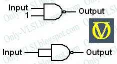
5. Give two ways of converting a two input NAND gate to an inverter.
Answer

6. Draw a Transmission Gate-based D-Latch.
Answer

7. Design a FSM which detects the sequence 10101 from a serial line without overlapping.
Answer

8. Design a FSM which detects the sequence 10101 from a serial line with overlapping.
Answer

9. Give the design of 8x1 multiplexer using 2x1 multiplexers.
Answer

10. Design a counter which counts from 1 to 10 ( Resets to 1, after 10 ).
Answer

Comments

Anonymous said…
For some questions answers are not there can you please post the answers also..?

Popular posts from this blog

Digital Design Interview Questions - All in 1

1. How do you convert a XOR gate into a buffer and a inverter (Use only one XOR gate for each)? Answer 2. Implement an 2-input AND gate using a 2x1 mux. Answer 3. What is a multiplexer? Answer A multiplexer is a combinational circuit which selects one of many input signals and directs to the only output. 4. What is a ring counter? Answer A ring counter is a type of counter composed of a circular shift register. The output of the last shift register is fed to the input of the first register. For example, in a 4-register counter, with initial register values of 1100, the repeating pattern is: 1100, 0110, 0011, 1001, 1100, so on. 5. Compare and Contrast Synchronous and Asynchronous reset. Answer Synchronous reset logic will synthesize to smaller flip-flops, particularly if the reset is gated with the logic generating the d-input. But in such a case, the combinational logic gate count grows, so the overall gate count savings may not be that significant. The clock works as a filter for sma...

XMR: Cross Module Reference

Cross Module Reference   Cross Module Reference abbreviated as XMR is a very useful concept in Verilog HDL (as well as system Verilog). However it seems to be less known among many users of Verilog. XMR is a mechanism built into Verilog to globally reference (i.e., across the modules) to any nets, tasks, functions etc. Using XMR, one can refer to any object of a module in any other module, irrespective of whether they are present below or above its hierarchy. Hence, a XMR can be a:   Downward reference OR Upward reference   Consider the following hierarchy:     Module A   Net x   Instance P of Module B     Net x   Instance M of Module D   Net x   Instance Q of Module C   Net x   Instance N of Module E    Net x   Instance R of Module B   Net x   Instance M of Module D   Net x ...

One-hot Encoding

Designing a FSM is the most common and challenging task for every digital logic designer. One of the key factors for optimizing a FSM design is the choice of state coding, which influences the complexity of the logic functions, the hardware costs of the circuits, timing issues, power usage, etc. There are several options like binary encoding, gray encoding, one-hot encoding, etc. The choice of the designer depends on the factors like technology, design specifications, etc. One-hot encoding In one-hot encoding only one bit of the state vector is asserted for any given state. All other state bits are zero. Thus if there are n states then n state flip-flops are required. As only one bit remains logic high and rest are logic low, it is called as One-hot encoding. Example : If there is a FSM, which has 5 states. Then 5 flip-flops are required to implement the FSM using one-hot encoding. The states will have the following values: S0 - 10000 S1 - 01000 S2 - 00100 S3 - 00010 S4 - 00001 Adv...