>> Introduction
>> The VLSI Design Flow
>> Importance of HDLs
>> Verilog HDL
>> Why Verilog ?
>> Digital Design Methods
Introduction
With the advent of VLSI technology and increased usage of digital circuits, designers has to design single chips with millions of transistors. It became almost impossible to verify these circuits of high complexity on breadboard. Hence Computer-aided techniques became critical for verification and design of VLSI digital circuits.As designs got larger and more complex, logic simulation assumed an important role in the design process. Designers could iron
out functional bugs in the architecture before the chip was designed further. All these factors which led to the evolution of Computer-Aided Digital Design, intern led to the emergence of Hardware Description Languages.
Verilog HDL and VHDL are the popular HDLs.Today, Verilog HDL is an accepted IEEE standard. In 1995, the original standard IEEE 1364-1995 was approved. IEEE 1364-2001 is the latest Verilog HDL standard that made significant improvements to the original standard.
The VLSI Design Flow
The VLSI IC circuits design flow is shown in the figure below. The various level of design are numbered and the gray coloured blocks show processes in the design flow.
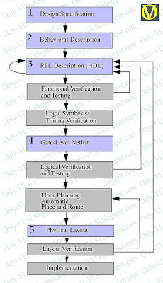 Specifications comes first, they describe abstractly the functionality, interface, and the architecture of the digital IC circuit to be designed.
Importance of HDLs
Verilog HDL
Verilog HDL is one of the most used HDLs. It can be used to describe designs at four levels of abstraction:
Why Verilog ?
Digital design methods
Digital design methods are of two types:
>> The VLSI Design Flow
>> Importance of HDLs
>> Verilog HDL
>> Why Verilog ?
>> Digital Design Methods
Introduction
With the advent of VLSI technology and increased usage of digital circuits, designers has to design single chips with millions of transistors. It became almost impossible to verify these circuits of high complexity on breadboard. Hence Computer-aided techniques became critical for verification and design of VLSI digital circuits.As designs got larger and more complex, logic simulation assumed an important role in the design process. Designers could iron
out functional bugs in the architecture before the chip was designed further. All these factors which led to the evolution of Computer-Aided Digital Design, intern led to the emergence of Hardware Description Languages.
Verilog HDL and VHDL are the popular HDLs.Today, Verilog HDL is an accepted IEEE standard. In 1995, the original standard IEEE 1364-1995 was approved. IEEE 1364-2001 is the latest Verilog HDL standard that made significant improvements to the original standard.
The VLSI Design Flow
The VLSI IC circuits design flow is shown in the figure below. The various level of design are numbered and the gray coloured blocks show processes in the design flow.
 Specifications comes first, they describe abstractly the functionality, interface, and the architecture of the digital IC circuit to be designed.
- Behavioral description is then created to analyze the design in terms of functionality, performance, compliance to given standards, and other specifications.
- RTL description is done using HDLs. This RTL description is simulated to test functionality. From here onwards we need the help of EDA tools.
- RTL description is then converted to a gate-level net list using logic synthesis tools. A gate-level netlist is a description of the circuit in terms of gates and connections between them, which are made in such a way that they meet the timing, power and area specifications.
- Finally a physical layout is made, which will be verified and then sent to fabrication.
Importance of HDLs
- RTL descriptions, independent of specific fabrication technology can be made an verified.
- functional verification of the design can be done early in the design cycle.
- Better representation of design due to simplicity of HDLs when compared to gate-level schematics.
- Modification and optimization of the design became easy with HDLs.
- Cuts down design cycle time significantly because the chance of a functional bug at a later stage in the design-flow is minimal.
Verilog HDL
Verilog HDL is one of the most used HDLs. It can be used to describe designs at four levels of abstraction:
- Algorithmic level.
- Register transfer level (RTL).
- Gate level.
- Switch level (the switches are MOS transistors inside gates).
Why Verilog ?
- Easy to learn and easy to use, due to its similarity in syntax to that of the C programming language.
- Different levels of abstraction can be mixed in the same design.
- Availability of Verilog HDL libraries for post-logic synthesis simulation.
- Most of the synthesis tools support Verilog HDL.
- The Programming Language Interface (PLI) is a powerful feature that allows the user to write custom C code to interact with the internal data structures of Verilog. Designers can customize a Verilog HDL simulator to their needs with the PLI.
Digital design methods
Digital design methods are of two types:
- Top-down design method : In this design method we first define the top-level block and then we build necessary sub-blocks, which are required to build the top-level block. Then the sub-blocks are divided further into smaller-blocks, and so on. The bottom level blocks are called as leaf cells. By saying bottom level it means that the leaf cell cannot be divided further.
- Bottom-up design method : In this design method we first find the bottom leaf cells, and then start building upper sub-blocks and building so on, we reach the top-level block of the design.
| << Previous | Home | Next >> |
Comments